
Introduction
Level of integrations in IC’s :

Source: wikipedia
ULSI, WSI, SoC and 3D-IC
- Conductor - Low Resistance
- SemiConductor - Resistance changes
- Insulator - High Resistance

Karl Ferdinand Braun developed the crystal detector, the first semiconductor device, in 1874.
SemiConductor
A semiconductor material has an electrical conductivity value falling between that if a conductor, such as metallic copper, and an insulator, such as glass.
Its conducting properties may be altered in useful ways by introducing impurities ("doping") .
Semiconductor - Types
Intrinsic (pure)
Extrinsic (Doped)
N type
Ptype
Intrinsic semiconductor | Donor atoms (n-Type Semiconductor) | Acceptor atoms (p-Type Semiconductor) | |
Group IV semiconductors | |||
Group III–V semiconductors | Aluminum phosphide, Aluminum arsenide, Gallium arsenide, Gallium nitride |
 “Transistor count doubling every 18 months “

If the MOSFET is normally OFF, and is turned ON by applying voltage at the gate terminal, then the MOSFET is known as enhancement-type MOSFET
If the MOSFET is normally ON, and is turned OFF by applying voltage at the gate terminal, then the MOSFET is known as depletion type MOSFET.


Each transistor consists of a stack of the conducting gate, an insulating layer of silicon dioxide (SiO2, better known as glass), and the silicon wafer, also called the substrate, body, or bulk.
Gate - M (metal / polysilicon)
Silicon dioxide - O - (SiO2)
Substrate -S- P type/N type
Transistor operation is controlled by electric fields so the devices are also called Metal Oxide Semiconductor Field Effect Transistors (MOSFETs) or simply FETs.
N MOS | P MOS |
P- Substrate connected to GND | N-Substrate connected to VDD |
N+ Source / Drain | P+ Source / Drain |
Source to Body & Drain to Body are Reverse Biased | Source to Body & Drain to Body are Reverse Biased |
Gate G Input =1 ON Gate G Input =0 OFF | Gate G Input =0 ON Gate G Input =1 OFF |
POWER SUPPLY RAILS : VDD - Logic 1
GND - Logic 0
If a voltage is applied at the gate terminal, a conducting channel is formed underneath the oxide layer between the source and drain.
A MOSFET is called n channel or simply nMOS when the channel is formed with electrons.
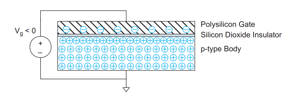
Depending on the voltage applied at the gate terminal, the operation of MOSFET is divided into three conditions:
Accumulation
Depletion
Inversion
✉️ These fixed negatively charged ions form the depletion layer.

✉️ If the positive gate voltage is large enough, the majority carrier holes are repelled into the substrate and the small numbers of minority carrier electrons are attracted towards the gate oxide surface.
✉️ The attracted electrons accumulate underneath the gate oxide layer and form a conducting path between the source and drain. This conducting path is called channel and the condition is known as “strong inversion”


Comments
Post a Comment